We all know that the HAL provides an abstraction of a standard system platform architecture. Driver developers use the HAL supplied interfaces to access the hardware, and by doing so almost all platform portability issues are managed by the HAL. An NT driver can usually be written once and built for all supported NT platforms without modification or conditional compilation.
However, in exchange for being a law-abiding NT driver developer, we expect that use of the HAL for access to hardware will not cause an enormous amount of overhead. Consider, for example, one of the simplest HAL interfaces: register access.
As you already know, the HAL register operations are designed to provide access from the kernel to 8, 16, or 32-bit addressable locations on peripheral devices. The register operations all have names such as:
READ_REGISTER_UCHAR
WRITE_REGISTER_ULONG
READ_REGISTER_BUFFER_USHORT
Use of register interface operations such as these is straightforward. Conceptually, these functions are simply doing pointer de-reference to access peripheral memory. Ignoring the HAL, we could consider register operations to look as follows:
//
// Our device has 2 8-bit registers located starting at
// PHYSICAL_ADDRESS_OF_REGISTER
//
PUCHAR RegisterPointer;
PHYSICAL_ADDRESS PhysicalAddress;
volatile UCHAR result;
//
// Initialize the 64bit physical address
//
PhysicalAddress.QuadPart = PHYSICAL_ADDRESS_OF_REGISTER;
//
// Translate the two bytes of physical address to a virtual address
//
RegisterPointer = MmMapIoSpace(PhysicalAddress, 2, FALSE);
//
// write the first register
//
*RegisterPointer = 0x1f;
//
// read the second register
//
result = RegisterPointer[1];
Through use of the HAL, we would expect that the register operations would be very lightweight. If accessing a register is simply pointer de-reference, then these operations ought to be no more than macros. HAL’s WRITE_REGISTER_UCHAR() interface ought to simply be something like:
#define WRITE_REGISTER_UCHAR( reg, val) \*(volatile UCHAR * const)(reg) = val;
Or perhaps the following would do if these just had to be functions:
__inline VOID WRITE_REGISTER_UCHAR( PUCHAR reg, UCHAR val) {*(volatile PUCHAR const) reg = val;
}
Why are Register Interface Operations implemented as Functions?
But why does the HAL provide a set of interfaces for accessing peripheral device registers in memory space at all if accessing peripheral device addresses is simply a matter of de-referencing a pointer?
The code segment shown above indicates that register operations could be expressed as simple portable C-language pointer dereference operations. Why should an NT kernel developer pay any attention at all to the HAL register operations?
Alas, the simple answer is cache coherency. The use of the HAL functions for register operations is warranted because some platforms have cache coherency issues (i.e., implementations that require that an explicit cache flush operation has to be performed to coax the data out of the IO cache and onto the peripheral device). It doesn’t do any good to toggle a bit on a control register on your peripheral device if the bit doesn’t actually get toggled because the write operation is sitting in cache!
As it turns out, this is an incomplete answer. My device registers can always be mapped to non-cached addresses, avoiding the cache issue, right? OK, so maybe there are some platforms where registers must be cached and an explicit IO cache flush operation must be performed. Indeed if we look at the MIPS or PPC implementation of WRITE_REGISTER_UCHAR:
#define WRITE_REGISTER_UCHAR(x, y) {\*(volatile UCHAR * const) (x) = y;\
KeFlushWriteBuffer();\
}
}
We can see that on some platforms, register operations do indeed require an explicit IO cache flush operation. Great, but this is implemented in the MIPS HAL (or perhaps I should say was implemented in the MIPS HAL,) as a simple lightweight macro. If I look through ntddk.h it is soon clear that the MIPS and PowerPC platforms use macros while Intel and Alpha use functions.
So I’m willing to make use of the portability features of the HAL for my kernel development, especially if the interface is low cost, and hides platform issues (such as requiring a KeFlushWriteBuffer(…) after each register write operation) as in the MIPS implementation. But as noted above, the Intel versions of these interfaces are all implemented as functions. The C language overhead for calling a function seems to be out of proportion for a very simple operation.
The ever-curious engineer wants to know what is going on with the Intel HAL. After all, it may be interesting how MIPS works, or how Alpha platforms operate, but what is critical is how the standard system platform operates (after all, a function call for every register access is expensive!). The temptation is to ignore the HAL and do the obvious — de-reference a pointer. You do so at your peril.
There is an interesting comment above the Intel HAL register function templates in ntddk.h (I find it interesting, your mileage may vary).
// The READ/WRITE_REGISTER_* calls manipulate I/O registers
// in MEMORY space. (Use x86 move instructions, with LOCK prefix
// to force correct behavior w.r.t. caches and write buffers.)
Well I don’t buy the "with respect to caches" part because the hardware provides cache coherency, and lock operations do not cause a cache flush. But how about the second part of that clause: "with respect to … write buffers?" What write buffers?
If you get out your copy of the Pentium Pro Family Developer’s Manual Volume 3: Operating System Writer’s Guide (if you don’t have a copy, Intel makes the Adobe PDF version available for download from their web site), and skip to Section 11.10 Write Buffer, we can clear all this up:
"The Pentium Pro processor temporarily stores each write (store) to memory in a write buffer.
The write buffer improves processor performance by allowing the processor to continue executing instructions without having to wait until a write to memory and/or to a cache is complete. It also allows writes to be delayed for more efficient use of memory-access bus cycles.
In general, the existence of the write buffer is transparent to software, even in systems that use multiple processors. The Pentium Pro processor ensures that write operations are always carried out in program order. It also insures that the contents of the write buffer are always drained to memory in the following situations:
• When an exception or interrupt is generated.
• When a serializing instruction is executed.
• When an I/O instruction is executed.
• When a locking operation is performed.
• When a BINIT operation is performed."
Oh, I see, the x86 architecture has yet another cache! This one is a FIFO of memory writes and is sort of cache coherent but is not exactly what the programmer expects when accessing peripheral devices.
Further research into the P6 architecture (Section 7.2 of the same manual) reveals that the P4, P5, and P6 all use write buffering but the P6 also allows read operations to be carried out "speculatively and in any order." In particular a read can be executed in advance (with respect to program order) of a write operation. The only guarantee is that a read to location X on a CPU is always going to be in program order with respect to writes to location X on that same CPU. On a single processor, writes are never re-ordered among themselves, and also on a single processor a read operation is guaranteed to return the value most recently written on that processor (meaning that speculative reads can be satisfied out of the write buffer).
On multiprocessor systems, all of the above applies to each CPU individually. However, there are no ordering of writes between processors other than the cache coherency rule, that each processor observes the same ordering of external writes (out of the internal write buffer into the memory cache subsystem) from any other processor.
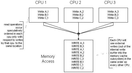
Figure 1 — Intel MP Write Ordering
In Figure 1 Intel MP Write Ordering, derived from the same Pentium Pro manual, the basic nature of write operations on an Intel Multiprocessor platform is depicted. For each processor, writes are ordered internally but are made visible to the other processors only as a result of the CPU controlled operation of its internal write buffer. The order in which writes to a specific memory location occur between processors is undefined, other than that each CPU observes the same external sequence of events.
The earlier comment cited from ntddk.h now starts to make sense. Controlling a peripheral device requires an ordered set of operations. The order must generally be the same from both the host system and the peripheral device perspective. If the host system writes to register 0x10 on a device to change the operational state of the device and then reads register 0x11 to see the results of that state change, it really is important to convince the CPU that the read cannot precede the write.
In our earlier example of register access using pointer de-reference, it is very probable that the peripheral device has not seen the write operation when the read operation occurs.
//
// write the first register
//
*RegisterPointer = 0x1f;
But where is the write? Is it in the CPU write buffer or on the device?
//
// read the second register
//
result = RegisterPointer[1];
If the contents of the second register on our device are determined by the values input to the first register, then the value of the result variable is correct (ignoring timing issues on the device itself) if, and only if, the CPU has actually written the specified value out to the first register on the target bus device. As we now know, on an Intel platform this is not predictable if we code the register operation as a simple pointer de-reference.
As the Intel manual indicates, there are ways to force the write buffer to be flushed out to physical memory. Interrupts, IN or OUT instructions, exceptions, lock instructions, etc. all force the CPU to flush the write buffer. The choice made by the NT Intel HAL, as implemented in the READ/WRITE_REGISTER_* interfaces, is to issue a non-destructive lock instruction to force register operations out to the peripheral device. This guarantees that the write is actually external to the CPU, and should in fact guarantee that the write has been delivered to the peripheral device.
Implications
It should be observed that on the Intel platform LOCK instructions are very expensive. Internally, the processor has to flush its write buffer (which is exactly what we want) and its instruction pipeline has to restart. Externally, the memory system bus is unavailable to any other component for the duration of the LOCK operation.
The cost of flushing the write buffer is difficult to calculate. First it depends on how full the buffer is, and how big it is (on the P5 it was 16 bytes, on the P6?). If the contents are all simply going to cache (except of course your bus operation) then the cost is relatively low. Uncached memory is clearly much more expensive that writing to cache, but pales in comparison to other bus I/O operations that might be in the write buffer.
What? Doesn’t everyone use the HAL register operations like they are supposed to? Well I have no idea, but that really wasn’t what I meant. Suppose that there is an ISA device with a shared memory buffer located on the device that is accessed using PIO (which is of course Intelese for using the CPU to copy data in and out of this buffer)? Writes from the CPU to that device using PIO are done using simple pointer de-reference operations and are consequently likely to be stacked up in the CPU write buffer. If you happen to be last in line behind a lot of 8Mhz ISA bus write operations, your register operation could take a very long time indeed.
Filling a register FIFO by calling WRITE_REGISTER_*() in a loop construct is a very expensive way to stuff data into your device. So instead you should of course use the WRITE_REGISTER_BUFFER_*() interface operations, as these will issue the LOCK instruction only after the buffer has been transferred, right?
Well that is exactly what you would think by reading the DDK documentation. However, a close examination of the WRITE_REGISTER_BUFFER_*() and READ_REGISTER_BUFFER_*() functions indicates that they in fact are buffer to buffer copy operations, not buffer to register copy operations.
The I/O Address Space equivalents of WRITE_REGISTER_BUFFER_*(), WRITE_PORT_BUFFER_*() behave exactly as one would think. They copy data from a buffer to a port address in I/O space. The register equivalents don’t. They increment both the buffer address and the register address on each loop iteration.
I personally found this unbelievable when it was brought to my attention. However, I offer as proof the PowerPC implementation of WRITE_REGISTER_BUFFER_ULONG() as documented in ntddk.h:
#define WRITE_REGISTER_BUFFER_ULONG(x, y, z) { \
PULONG registerBuffer = x; \
PULONG writeBuffer = y; \
ULONG writeCount; \
for (writeCount = z; \
writeCount--; \
writeBuffer++, registerBuffer++) { \
*(volatile ULONG * const)(registerBuffer) = *writeBuffer; \
} \
KeFlushWriteBuffer(); \
}
So this is interesting. It almost looks as if at some point in time the register buffer operations were redefined in order to resolve a minor problem with PIO on Intel devices. What minor problem? The minor problem is that the Write Buffer caching on the CPU (the straight forward approach to PIO of simply doing pointer de-reference in a loop), has left an indeterminate amount of data in the CPU, not on the device. So instead one can apparently use WRITE_REGISTER_BUFFER_*(), pretending that your shared memory buffer on the peripheral device is a register, and at the end of the copy loop, the HAL will force a CPU Write Buffer flush.
Note, if you look at your hardware programmer’s guide for your peripheral device and it says something like, "Data transfer to the Acme Internet Toaster Device is accomplished by 32-bit write operations to the data FIFO located at register address 0x1000," then you have a problem. If you use the NT DDK as documented, you are going to write one 32bit value to register 0x1000 and the rest of your data is going to cause some unspecified behavior. If you call WRITE_REGISTER_ULONG() inside a loop, you pay the cost of a LOCK operation on each iteration. If you do the obvious, and simply do pointer deference inside the loop, followed by a single WRITE_REGISTER_ULONG() operation outside the loop, your code is correct and efficient but potentially non-portable as you are accessing registers without using the prescribed HAL interface. See the following:
__inline void WriteRegisterBufferUlong(PULONG dataFifo,
PULONG buffer,
ULONG length)
{
if (length == 0) {
//
// avoid callers trying to transfer
// zero bytes of data
//
return;
}
while (length-- > 1) {
//
// Oh well…
//
*(volatile ULONG * const) dataFifo = *buffer++;
}
//
// Convince the most likely platform that the
// data really ought to be outside the CPU.
//
WRITE_REGISTER_ULONG(dataFifo, *buffer);
}
Law-abiding or not, driver writers interacting with the HAL best be careful. Often times, it won’t ever come down to which is the correct way to access hardware – more likely it’ll be the more correct way for a particular device in a particular instance. Good luck!


 Post Your Comment
